


Images are for reference only See Product Specifications
Orders Over
$5000
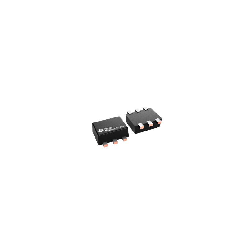
74LVC1T45GW,125

Dual supply translating transceiver; 3-state


Brands: Nexperia
Mfr.Part #: 74LVC1T45GW,125
Datasheet: 74LVC1T45GW,125 Datasheet (PDF)
Package/Case: TSSOP-6
RoHS Status:
Stock Condition: 6,303 pcs, New Original
Product Type: Translators, Level Shifters
Warranty: 1 Year Ovaga Warranty - Find Out More
0
1
*All prices are in USD
| Qty | Unit Price | Ext Price |
|---|---|---|
| 5 | $0.182 | $0.910 |
| 50 | $0.145 | $7.250 |
| 150 | $0.129 | $19.350 |
| 500 | $0.110 | $55.000 |
| 3000 | $0.101 | $303.000 |
| 6000 | $0.095 | $570.000 |
In Stock: 6,303 PCS
74LVC1T45GW,125 General Description
One of the key features of the 74LVC1T45GW,125 is its partial power-down capability using the I circuitry. This ensures that the output is disabled during power-down, preventing any harmful backflow current through the device. Additionally, the active bus hold circuitry in the 74LVCH1T45 ensures that unused data inputs are held at a valid logic level, providing reliable operation even in scenarios where data inputs are floating
Features
- Wide supply voltage range:VCC(A): 1.2 V to 5.5 VVCC(B): 1.2 V to 5.5 V
- VCC(A): 1.2 V to 5.5 V
- VCC(B): 1.2 V to 5.5 V
- High noise immunity
- Maximum data rates:420 Mbps (3.3 V to 5.0 V translation)210 Mbps (translate to 3.3 V))140 Mbps (translate to 2.5 V)75 Mbps (translate to 1.8 V)60 Mbps (translate to 1.5 V)
- 420 Mbps (3.3 V to 5.0 V translation)
- 210 Mbps (translate to 3.3 V))
- 140 Mbps (translate to 2.5 V)
- 75 Mbps (translate to 1.8 V)
- 60 Mbps (translate to 1.5 V)
- Suspend mode
- Latch-up performance exceeds 100 mA per JESD 78 Class II
- ±24 mA output drive (VCC = 3.0 V)
- Inputs accept voltages up to 5.5 V
- Low power consumption: 16 μA maximum ICC
- IOFF circuitry provides partial Power-down mode operation
- Complies with JEDEC standards:JESD8-7 (1.2 V to 1.95 V)JESD8-5 (1.8 V to 2.7 V)JESD8C (2.7 V to 3.6 V)JESD36 (4.5 V to 5.5 V)
- JESD8-7 (1.2 V to 1.95 V)
- JESD8-5 (1.8 V to 2.7 V)
- JESD8C (2.7 V to 3.6 V)
- JESD36 (4.5 V to 5.5 V)
- ESD protection:HBM: ANSI/ESDA/JEDEC JS-001 class 3A exceeds 4000 VCDM: ANSI/ESDA/JEDEC JS-002 class C3 exceeds 1000 V
- HBM: ANSI/ESDA/JEDEC JS-001 class 3A exceeds 4000 V
- CDM: ANSI/ESDA/JEDEC JS-002 class C3 exceeds 1000 V
- Multiple package options
- Specified from -40 °C to +85 °C and -40 °C to +125 °C
Specifications
| Parameter | Value | Parameter | Value |
|---|---|---|---|
| Type number | 74LVC1T45GW | Product status | Production |
| VCC(A) (V) | 1.2 - 5.5 | VCC(B) (V) | 1.2 - 5.5 |
| Logic switching levels | CMOS/LVTTL | Output drive capability (mA) | ± 24 |
| tpd (ns) | 2.5 | Nr of bits | 1 |
| Power dissipation considerations | low | Tamb (°C) | -40~125 |
| Rth(j-a) (K/W) | 268 | Ψth(j-top) (K/W) | 41.4 |
| Rth(j-c) (K/W) | 156 | Package name | TSSOP6 |
| Packing | SOT363-2_125 | Orderable part number | 74LVC1T45GW,125 |
| Chemical content | 74LVC1T45GW |
Shipping
| Shipping Type | Ship Fee | Lead Time | |
|---|---|---|---|
 |
DHL | $20.00-$40.00 (0.50 KG) | 2-5 days |
 |
Fedex | $20.00-$40.00 (0.50 KG) | 2-5 days |
 |
UPS | $20.00-$40.00 (0.50 KG) | 2-5 days |
 |
TNT | $20.00-$40.00 (0.50 KG) | 2-5 days |
 |
EMS | $20.00-$40.00 (0.50 KG) | 2-5 days |
 |
REGISTERED AIR MAIL | $20.00-$40.00 (0.50 KG) | 2-5 days |
Processing Time:Shipping fee depend on different zone and country.
Payment
| Terms of payment | Hand Fee | |
|---|---|---|
 |
Wire Transfer | charge US$30.00 banking fee. |
 |
Paypal | charge 4.0% service fee. |
 |
Credit Card | charge 3.5% service fee. |
 |
Western Union | charge US.00 banking fee. |
 |
Money Gram | charge US$0.00 banking fee. |
Guarantees
1.The electronic components you purchase include 365 Days Warranty, We guarantee product quality.
2.If some of the items you received aren't of perfect quality, we would resiponsibly arrange your refund or replacement. But the items must remain their orginal condition.
Packing
-

Step1 :Product
-

Step2 :Vacuum packaging
-

Step3 :Anti-static bag
-

Step4 :Individual packaging
-

Step5 :Packaging boxes
-

Step6 :bar-code shipping tag


All the products will packing in anti-staticbag. Ship with ESD antistatic protection.
Outside ESD packing’s lable will use ourcompany’s information: Part Mumber, Brand and Quantity.
We will inspect all the goods before shipment,ensure all the products at good condition and ensure the parts are new originalmatch datasheet.
After all the goods are ensure no problems afterpacking, we will packing safely and send by global express. It exhibitsexcellent puncture and tear resistance along with good seal integrity.


Part points
-
The 74LVC1T45GW,125 chip is a single-bit dual supply level translator designed for translating voltage levels in mixed-mode applications. It features an auto-direction sensing circuit that eliminates the need for a direction control signal. The chip operates at a voltage range of 1.65V to 5.5V, making it suitable for a wide range of applications that require voltage level translation.
-
Equivalent
Some equivalent products of the 74LVC1T45GW,125 chip are SN74LVC1T45DBVR, CD74HCT245E, NC7S245P5X, and LTC4300-2IMS8#PBF. These are all voltage level translators and buffers that perform similar functions to the 74LVC1T45GW,125 chip. -
Features
The 74LVC1T45GW,125 is a single-bit dual-supply bus buffer that features a wide voltage range (1.65V to 5.5V), high-speed operation (up to 5.0ns propagation delay), and supports mixed-voltage environments. It also has 5V tolerant inputs and outputs and provides bidirectional level shifting without a direction control signal. -
Pinout
The 74LVC1T45GW,125 is a single-bit dual-supply bidirectional voltage level translator. It has a pin count of 6 and can be used to translate logic signals between different voltage levels, such as between 1.8V and 3.3V. -
Manufacturer
The manufacturer of the 74LVC1T45GW,125 is NXP Semiconductors. NXP Semiconductors is a global semiconductor company that designs and produces a wide range of products used in various industries such as automotive, security, and mobile devices. They are known for their high-quality and innovative semiconductor solutions. -
Application Field
The 74LVC1T45GW,125 is commonly used in applications such as automotive, industrial control, consumer electronics, and communication systems. It is ideal for bidirectional level shifting, voltage translation, and buffering signals between devices with different voltage levels. -
Package
The 74LVC1T45GW,125 chip is a digital buffer/line driver with 3-state output in a surface-mount SC-88A (SOT353) package. It has a size of 2mm x 1.25mm x 1.05mm.


We provide high quality products, thoughtful service and after sale guarantee
-

We have rich products, can meet your various needs.
-

Minimum order quantity starts from 1pcs.
-

Lowest international shipping fee starts from $0.00
-

365 days quality guarantee for all products


