


Images are for reference only See Product Specifications
Orders Over
$5000CY7B923-JXI
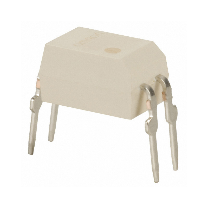
28-pin PLCC package


Brands: Infineon
Mfr.Part #: CY7B923-JXI
Datasheet: CY7B923-JXI Datasheet (PDF)
Package/Case: PLCC-28
Product Type: Drivers, Receivers, Transceivers
RoHS Status:
Stock Condition: 5,889 pcs, New Original
Warranty: 1 Year Ovaga Warranty - Find Out More
0
1
CY7B923-JXI General Description
Featuring two fully independent UART channels and an integrated DPLL, the CY7B923-JXI is designed to enhance data communication with advanced functionality. Automatic baud rate detection, on-chip hardware flow control, and energy-conserving power-down modes further contribute to its efficiency and versatility. Whether used in industrial automation, telecommunications, or data acquisition systems, this dual UART provides high-speed data transfer and reliable performance to meet the requirements of various communication applications
Features
- This synchronous FIFO memory device is designed for use in embedded systems applications
- The CY7B923-JXI features high-speed data transfer rates and low power consumption
- It includes dual clocking schemes and bus matching logic for easy integration
Application
- Skew PLL technology
- Programmable clock distribution
- Switches and routers
Specifications
| Parameter | Value | Parameter | Value |
|---|---|---|---|
| Product Category | Telecom Interface ICs | RoHS | Details |
| Product | HOTLink Transceivers | Supply Voltage - Max | 4.5 V |
| Supply Voltage - Min | 4.5 V | Minimum Operating Temperature | - 40 C |
| Maximum Operating Temperature | + 85 C | Mounting Style | SMD/SMT |
| Package / Case | PLCC-28 | Brand | Infineon Technologies |
| Moisture Sensitive | Yes | Number of Channels | 1 Channel |
| Product Type | Telecom Interface ICs | Series | CY7B923 |
| Factory Pack Quantity | 74 | Subcategory | Interface ICs |
| Unit Weight | 0.041719 oz |
Shipping
| Shipping Type | Ship Fee | Lead Time | |
|---|---|---|---|
 |
DHL | $20.00-$40.00 (0.50 KG) | 2-5 days |
 |
Fedex | $20.00-$40.00 (0.50 KG) | 2-5 days |
 |
UPS | $20.00-$40.00 (0.50 KG) | 2-5 days |
 |
TNT | $20.00-$40.00 (0.50 KG) | 2-5 days |
 |
EMS | $20.00-$40.00 (0.50 KG) | 2-5 days |
 |
REGISTERED AIR MAIL | $20.00-$40.00 (0.50 KG) | 2-5 days |
Processing Time:Shipping fee depend on different zone and country.
Payment
| Terms of payment | Hand Fee | |
|---|---|---|
 |
Wire Transfer | charge US$30.00 banking fee. |
 |
Paypal | charge 4.0% service fee. |
 |
Credit Card | charge 3.5% service fee. |
 |
Western Union | charge US.00 banking fee. |
 |
Money Gram | charge US$0.00 banking fee. |
Guarantees
1.The electronic components you purchase include 365 Days Warranty, We guarantee product quality.
2.If some of the items you received aren't of perfect quality, we would resiponsibly arrange your refund or replacement. But the items must remain their orginal condition.
Packing
-

Step1 :Product
-

Step2 :Vacuum packaging
-

Step3 :Anti-static bag
-

Step4 :Individual packaging
-

Step5 :Packaging boxes
-

Step6 :bar-code shipping tag


All the products will packing in anti-staticbag. Ship with ESD antistatic protection.
Outside ESD packing’s lable will use ourcompany’s information: Part Mumber, Brand and Quantity.
We will inspect all the goods before shipment,ensure all the products at good condition and ensure the parts are new originalmatch datasheet.
After all the goods are ensure no problems afterpacking, we will packing safely and send by global express. It exhibitsexcellent puncture and tear resistance along with good seal integrity.


Part points
-
The CY7B923-JXI is a high-speed synchronous dual-port RAM chip designed for networking and telecommunications applications. It features 4K x 9 dual-port RAM configuration, 65 MHz operation, and a low access time of 6.5 ns. Its dual-port design allows for simultaneous access from two separate devices, making it ideal for high-performance data transfer applications.
-
Equivalent
The equivalent products of CY7B923-JXI chip are MC10H136, AM26LS32, and MC74HCT32A. -
Features
- CY7B923-JXI is a high-performance PLL clock generator - It has 3 independent PLLs with programmable frequency synthesis - Offers 150 ps peak-to-peak jitter performance - It has dual differential outputs - Has a wide operating frequency range from 8 kHz to 133 MHz - Offers skew control for output synchronization -
Pinout
The CY7B923-JXI is a 24-pin parallel input to serial output shift register IC. It has data inputs (D0-D7), clock inputs (CLK and SH/LD), serial output (QH), and control inputs for shift/load operation. It is commonly used in systems that require serial data transfer and parallel data conversion. -
Manufacturer
Cypress Semiconductor Corporation is the manufacturer of CY7B923-JXI. It is a leading American semiconductor design and manufacturing company specializing in high-performance integrated circuits and embedded system solutions. -
Application Field
CY7B923-JXI is commonly used in telecommunications, networking equipment, and industrial automation applications. It is suitable for timing and clock distribution tasks that require low-skew clock signals, such as in high-speed data communication systems, processors, switches, routers, and other digital devices. -
Package
The CY7B923-JXI chip comes in a 24-pin SOIC (Small Outline Integrated Circuit) package, with a JEDEC standard form factor. It measures 0.300 inches wide and 0.505 inches long, making it a compact and easily integrated integrated circuit.


We provide high quality products, thoughtful service and after sale guarantee
-

We have rich products, can meet your various needs.
-

Minimum order quantity starts from 1pcs.
-

Lowest international shipping fee starts from $0.00
-

365 days quality guarantee for all products


