

Images are for reference only See Product Specifications
Orders Over
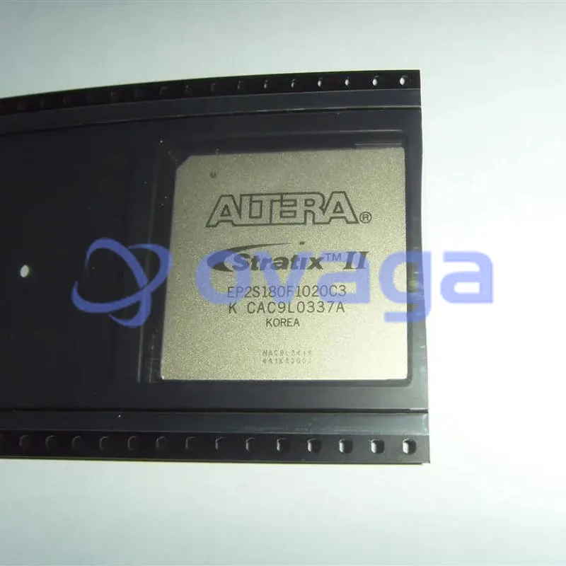
$5000EP2S180F1020C3
With its Field Programmable Gate Array technology, the EP2S180F1020C3 offers customizable solutions for complex designs


Brands: ALTERA CORP
Mfr.Part #: EP2S180F1020C3
Datasheet: EP2S180F1020C3 Datasheet (PDF)
Package/Case: FBGA-1020
Product Type: FPGAs (Field Programmable Gate Array)
RoHS Status:
Stock Condition: 6,554 pcs, New Original
Warranty: 1 Year Ovaga Warranty - Find Out More
0
1
EP2S180F1020C3 General Description
Boasting a 180,000 logic element capacity and a C3 speed grade, the EP2S180F1020C3 is a formidable Altera Stratix II FPGA designed for high-performance processing. With 1,020 pins and a wide range of I/O options, this FPGA is equipped to handle complex logic functions, high-speed data processing, and real-time signal processing across various industries. Its support for embedded memory blocks, high-speed transceivers, and flexible routing resources ensures that it can meet the demanding requirements of modern applications
Features
- The Stratix II family offers the following
- features:
- 15,600 to 179,400 equivalent LEs; see Table 1–1
- New and innovative adaptive logic module (ALM), the basic building block of the Stratix II architecture, maximizes performance and resource usage efficiency
- Up to 9,383,040 RAM bits (1,172,880 bytes) available without reducing logic resources
- TriMatrix memory consisting of three RAM block sizes to implement true dual-port memory and first-in first-out (FIFO) buffers
- High-speed DSP blocks provide dedicated implementation of multipliers (at up to 450 MHz), multiply-accumulate functions, and finite impulse response (FIR) filters
- Up to 16 global clocks with 24 clocking resources per device region
- Clock control blocks support dynamic clock network enable/disable, which allows clock networks to power down to reduce power consumption in user mode
- Up to 12 PLLs (four enhanced PLLs and eight fast PLLs) per device provide spread spectrum, programmable bandwidth, clock switchover, real-time PLL reconfiguration, and advanced multiplication and phase shifting
- Support for numerous single-ended and differential I/O standards
- High-speed differential I/O support with DPA circuitry for 1-Gbps performance
- Support for high-speed networking and communications bus standards including Parallel RapidIO, SPI-4 Phase 2 (POS-PHY Level 4), HyperTransport™ technology, and SFI-4
- Support for high-speed external memory, including DDR and DDR2 SDRAM, RLDRAM II, QDR II SRAM, and SDR SDRAM
- Support for multiple intellectual property megafunctions from Altera MegaCore® functions and Altera Megafunction Partners Program (AMPPSM) megafunctions
- Support for design security using configuration bitstream encryption
- Support for remote configuration updates
Specifications
| Parameter | Value | Parameter | Value |
|---|---|---|---|
| Pbfree Code | No | Rohs Code | No |
| Part Life Cycle Code | Transferred | Ihs Manufacturer | ALTERA CORP |
| Part Package Code | BGA | Package Description | 33 X 33 MM, 1 MM PITCH, FBGA-1020 |
| Pin Count | 1020 | Reach Compliance Code | not_compliant |
| HTS Code | 8542.39.00.01 | Clock Frequency-Max | 717 MHz |
| Combinatorial Delay of a CLB-Max | 4.672 ns | JESD-30 Code | S-PBGA-B1020 |
| JESD-609 Code | e0 | Length | 33 mm |
| Moisture Sensitivity Level | 4 | Number of CLBs | 71760 |
| Number of Inputs | 742 | Number of Logic Cells | 179400 |
| Number of Outputs | 734 | Number of Terminals | 1020 |
| Operating Temperature-Max | 85 °C | Operating Temperature-Min | |
| Organization | 71760 CLBS | Package Body Material | PLASTIC/EPOXY |
| Package Code | BGA | Package Equivalence Code | BGA1020,32X32,40 |
| Package Shape | SQUARE | Package Style | GRID ARRAY |
| Peak Reflow Temperature (Cel) | 220 | Power Supplies | 1.2,1.5/3.3,3.3 V |
| Programmable Logic Type | FIELD PROGRAMMABLE GATE ARRAY | Qualification Status | Not Qualified |
| Seated Height-Max | 3.5 mm | Supply Voltage-Max | 1.25 V |
| Supply Voltage-Min | 1.15 V | Supply Voltage-Nom | 1.2 V |
| Surface Mount | YES | Technology | CMOS |
| Temperature Grade | OTHER | Terminal Finish | TIN LEAD |
| Terminal Form | BALL | Terminal Pitch | 1 mm |
| Terminal Position | BOTTOM | Time@Peak Reflow Temperature-Max (s) | 20 |
| Width | 33 mm |
Shipping
| Shipping Type | Ship Fee | Lead Time | |
|---|---|---|---|
 |
DHL | $20.00-$40.00 (0.50 KG) | 2-5 days |
 |
Fedex | $20.00-$40.00 (0.50 KG) | 2-5 days |
 |
UPS | $20.00-$40.00 (0.50 KG) | 2-5 days |
 |
TNT | $20.00-$40.00 (0.50 KG) | 2-5 days |
 |
EMS | $20.00-$40.00 (0.50 KG) | 2-5 days |
 |
REGISTERED AIR MAIL | $20.00-$40.00 (0.50 KG) | 2-5 days |
Processing Time:Shipping fee depend on different zone and country.
Payment
| Terms of payment | Hand Fee | |
|---|---|---|
 |
Wire Transfer | charge US$30.00 banking fee. |
 |
Paypal | charge 4.0% service fee. |
 |
Credit Card | charge 3.5% service fee. |
 |
Western Union | charge US.00 banking fee. |
 |
Money Gram | charge US$0.00 banking fee. |
Guarantees
1.The electronic components you purchase include 365 Days Warranty, We guarantee product quality.
2.If some of the items you received aren't of perfect quality, we would resiponsibly arrange your refund or replacement. But the items must remain their orginal condition.
Packing
-

Step1 :Product
-

Step2 :Vacuum packaging
-

Step3 :Anti-static bag
-

Step4 :Individual packaging
-

Step5 :Packaging boxes
-

Step6 :bar-code shipping tag


All the products will packing in anti-staticbag. Ship with ESD antistatic protection.
Outside ESD packing’s lable will use ourcompany’s information: Part Mumber, Brand and Quantity.
We will inspect all the goods before shipment,ensure all the products at good condition and ensure the parts are new originalmatch datasheet.
After all the goods are ensure no problems afterpacking, we will packing safely and send by global express. It exhibitsexcellent puncture and tear resistance along with good seal integrity.


Part points
-
The EP2S180F1020C3 chip is a field-programmable gate array (FPGA) made by Altera Corporation. It offers high functionality and flexibility for designing and implementing digital circuits. With 180,000 logic elements, 4,040 Kbits of embedded memory, and advanced features like high-speed transceivers, it is suitable for a wide range of applications including telecommunications, industrial automation, and image and signal processing.
-
Equivalent
The equivalent products of EP2S180F1020C3 chip from Altera are Arria II GX FPGAs. -
Features
The EP2S180F1020C3 is a field-programmable gate array (FPGA) manufactured by Altera. It has 180,000 logic elements, 5,808 kilobits of embedded memory, and supports up to 1,280 user I/O pins. It operates at a maximum frequency of 419 MHz and includes built-in transceivers for high-speed data communication. -
Pinout
The EP2S180F1020C3 is an FPGA with 1020 pins. The pins serve various functions such as input/output (I/O), clock inputs, power supply, configuration, and debugging purposes. -
Manufacturer
EP2S180F1020C3 is manufactured by Altera Corporation. Altera is a company that specializes in designing, manufacturing, and selling programmable logic devices. This specific model is a field-programmable gate array (FPGA) manufactured by Altera for use in various electronic applications. -
Application Field
The EP2S180F1020C3 is a field programmable gate array (FPGA) with 180,000 logic elements. It is commonly used in a wide range of applications, including telecommunications, video and image processing, network processing, high-performance computing, industrial control, and automotive electronics. -
Package
The EP2S180F1020C3 chip comes in a Ball Grid Array (BGA) package type. It has a form factor of 1020 pins and a size of 31mm x 31mm.


We provide high quality products, thoughtful service and after sale guarantee
-

We have rich products, can meet your various needs.
-

Minimum order quantity starts from 1pcs.
-

Lowest international shipping fee starts from $0.00
-

365 days quality guarantee for all products


