


Images are for reference only See Product Specifications
Orders Over
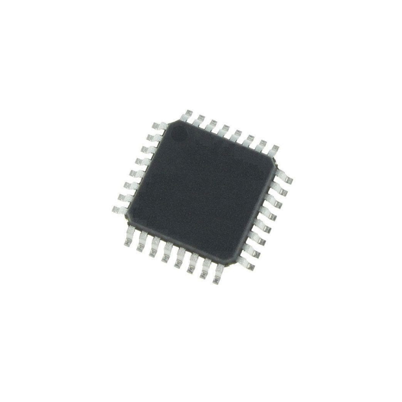
$5000MC56F8035V
16-bitDigitalSignalControllers


Brands: Freescale / NXP
Mfr.Part #: MC56F8035V
Datasheet: MC56F8035V Datasheet (PDF)
Package/Case: QFP-44
RoHS Status:
Stock Condition: 6,554 pcs, New Original
Warranty: 1 Year Ovaga Warranty - Find Out More
0
1
MC56F8035V General Description
The MC56F8035V is a microcontroller from NXP Semiconductors. It is part of the MC56F8000 series and features a 16-bit digital signal controller (DSC) core. The MC56F8035V includes peripherals and interfaces that are commonly used in embedded control applications.
Features
- Digital Signal Controller Core
- Efficient 16-bit 56800E family Digital Signal Controller (DSC) engine with dual Harvard architecture
- As many as 32 Million Instructions Per Second (MIPS) at 32MHz core frequency
- Single-cycle 16 × 16-bit parallel Multiplier-Accumulator (MAC)
- Four 36-bit accumulators, including extension bits
- 32-bit arithmetic and logic multi-bit shifter
- Parallel instruction set with unique DSP addressing modes
- Hardware DO and REP loops
- Three internal address buses
- Four internal data buses
- Instruction set supports both DSP and controller functions
- Controller-style addressing modes and instructions for compact code
- Efficient C compiler and local variable support
- Software subroutine and interrupt stack with depth limited only by memory
- JTAG/Enhanced On-Chip Emulation (OnCE) for unobtrusive, processor speed-independent real-time debugging
- Memory
- Dual Harvard architecture permits as many as three simultaneous accesses to program and data memory
- Flash security and protection that prevent unauthorized users from gaining access to the internal Flash
- On-chip memory
- — 64KB of Program Flash (56F80235 device)
- 32KB of Program Flash (56F8025 device)
- — 8KB of Unified Data/Program RAM (56F8035 device)
- 4KB of Unified Data/Program RAM (56F8025 device)
- EEPROM emulation capability using Flash
- Peripheral Circuits for 56F8035/56F8025
- One multi-function six-output Pulse Width Modulator (PWM) module
- — Up to 96MHz PWM operating clock
- — 15 bits of resolution
- — Center-aligned and edge-aligned PWM signal mode
- — Four programmable fault inputs with programmable digital filter
- — Double-buffered PWM registers
- — Each complementary PWM signal pair allows selection of a PWM supply source from:
- – PWM generator
- – External GPIO
- – Internal timers
- – Analog comparator outputs
- – ADC conversion result which compares with values of ADC high- and low-limit registers to set PWM output
- Two independent 12-bit Analog-to-Digital Converters (ADCs)
- — 2 x 4 channel inputs
- — Supports both simultaneous and sequential conversions
- — ADC conversions can be synchronized by both PWM and timer modules
- — Sampling rate up to 2.67MSPS
- — 16-word result buffer registers
- Two internal 12-bit Digital-to-Analog Converters (DACs)
- — 2 microsecond settling time when output swing from rail to rail
- — Automatic waveform generation generates square, triangle and sawtooth waveforms with
- programmable period, update rate, and range
- One 16-bit multi-purpose Quad Timer module (TMR)
- — Up to 96MHz operating clock
- — Eight independent 16-bit counter/timers with cascading capability
- — Each timer has capture and compare capability
- — Up to 12 operating modes
- One Queued Serial Communication Interface (QSCI) with LIN Slave functionality
- — Full-duplex or single-wire operation
- — Two receiver wake-up methods:
- – Idle line
- – Address mark
- — Four-bytes-deep FIFOs are available on both transmitter and receiver
- One Queued Serial Peripheral Interfaces (QSPI)
- — Full-duplex operation
- — Master and slave modes
- — Four-words-deep FIFOs available on both transmitter and receiver
- — Programmable Length Transactions (2 to 16 bits)
- One Inter-Integrated Circuit (I2C) port
- — Operates up to 400kbps
- — Supports both master and slave operation
- — Supports both 10-bit address mode and broadcasting mode
- Three 16-bit Programmable Interval Timers (PITs)
- Two analog Comparators (CMPs)
- — Selectable input source includes external pins, DACs
- — Programmable output polarity
- — Output can drive Timer input, PWM fault input, PWM source, external pin output and trigger ADCs
- — Output falling and rising edge detection able to generate interrupts
- Computer Operating Properly (COP)/Watchdog timer capable of selecting different clock sources
- Up to 35 General-Purpose I/O (GPIO) pins with 5V tolerance
- Integrated Power-On Reset (POR) and Low-Voltage Interrupt (LVI) module
- Phase Lock Loop (PLL) provides a high-speed clock to the core and peripherals
- Clock sources:
- — On-chip relaxation oscillator
- — External clock: Crystal oscillator, ceramic resonator, and external clock source
- JTAG/EOnCE debug programming interface for real-time debugging
- Energy Information
- Fabricated in high-density CMOS with 5V tolerance
- On-chip regulators for digital and analog circuitry to lower cost and reduce noise
- Wait and Stop modes available
- ADC smart power management
- Each peripheral can be individually disabled to save power
Application
- The MC56F8035V is suitable for a wide range of applications, including:
- Motor control systems
- Power management applications
- Industrial automation
- Sensor interfacing and data acquisition
- Consumer electronics
Specifications
| Parameter | Value | Parameter | Value |
|---|---|---|---|
| Product Name | MC56F8035V | Product Type | Microcontroller |
| Manufacturer | NXP | Core Processor | 56F8xx |
| Core Size | 16-Bit | Speed | 50MHz |
| Connectivity | CAN, I²C, LIN, SPI, UART/USART | Peripherals | ADC, DMA, POR, PWM, WDT |
| Number of I/Os | 64 | Program Memory Size | 128KB (128K x 8) |
| Data RAM Size | 8KB | Voltage - Supply | 1.8 V ~ 3.6 V |
| Operating Temperature | -40°C ~ 105°C | Mounting Type | Surface Mount |
| Package / Case | 64-LQFP |
Shipping
| Shipping Type | Ship Fee | Lead Time | |
|---|---|---|---|
 |
DHL | $20.00-$40.00 (0.50 KG) | 2-5 days |
 |
Fedex | $20.00-$40.00 (0.50 KG) | 2-5 days |
 |
UPS | $20.00-$40.00 (0.50 KG) | 2-5 days |
 |
TNT | $20.00-$40.00 (0.50 KG) | 2-5 days |
 |
EMS | $20.00-$40.00 (0.50 KG) | 2-5 days |
 |
REGISTERED AIR MAIL | $20.00-$40.00 (0.50 KG) | 2-5 days |
Processing Time:Shipping fee depend on different zone and country.
Payment
| Terms of payment | Hand Fee | |
|---|---|---|
 |
Wire Transfer | charge US$30.00 banking fee. |
 |
Paypal | charge 4.0% service fee. |
 |
Credit Card | charge 3.5% service fee. |
 |
Western Union | charge US.00 banking fee. |
 |
Money Gram | charge US$0.00 banking fee. |
Guarantees
1.The electronic components you purchase include 365 Days Warranty, We guarantee product quality.
2.If some of the items you received aren't of perfect quality, we would resiponsibly arrange your refund or replacement. But the items must remain their orginal condition.
Packing
-

Step1 :Product
-

Step2 :Vacuum packaging
-

Step3 :Anti-static bag
-

Step4 :Individual packaging
-

Step5 :Packaging boxes
-

Step6 :bar-code shipping tag


All the products will packing in anti-staticbag. Ship with ESD antistatic protection.
Outside ESD packing’s lable will use ourcompany’s information: Part Mumber, Brand and Quantity.
We will inspect all the goods before shipment,ensure all the products at good condition and ensure the parts are new originalmatch datasheet.
After all the goods are ensure no problems afterpacking, we will packing safely and send by global express. It exhibitsexcellent puncture and tear resistance along with good seal integrity.


We provide high quality products, thoughtful service and after sale guarantee
-

We have rich products, can meet your various needs.
-

Minimum order quantity starts from 1pcs.
-

Lowest international shipping fee starts from $0.00
-

365 days quality guarantee for all products


Recommend
-
![S3C2410A-20]()
-
![MB86290A]()
-
![HD61830A00]()
-
![HD44780A00]()
-
![SED1354F0A]()
-
![T65550B]()
CHIPS


