

Images are for reference only See Product Specifications
Orders Over
$5000
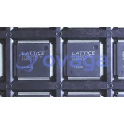
LATTICE LFE3-35EA-8FN484C

LFE3-35EA-8FN484C 1.2V 484-Pin FBGA


Brands: Lattice
Mfr.Part #: LFE3-35EA-8FN484C
Datasheet: LFE3-35EA-8FN484C Datasheet (PDF)
Package/Case: FPBGA-484
RoHS Status:
Stock Condition: 9,458 pcs, New Original
Product Type: FPGAs (Field Programmable Gate Array)
Warranty: 1 Year Ovaga Warranty - Find Out More
0
1
*All prices are in USD
| Qty | Unit Price | Ext Price |
|---|---|---|
| 1 | $30.216 | $30.216 |
| 200 | $11.695 | $2339.000 |
| 500 | $11.284 | $5642.000 |
| 1000 | $11.079 | $11079.000 |
In Stock: 9,458 PCS
LFE3-35EA-8FN484C General Description
The LFE3-35EA-8FN484C FPGA, part of the ECP3 family from Lattice Semiconductor, is an ideal choice for designers looking for a high-performance, yet power-efficient platform for their applications. Its combination of advanced features, such as multiple I/O standards, high-speed SERDES channels, and embedded memory blocks, makes it well-suited for a wide range of use cases. Whether it's data processing in telecommunications, networking, industrial automation, or medical imaging, this FPGA offers the right balance of capabilities to address the demands of modern electronic designs
Features
- Higher Logic Density for Increased System Integration
- 17K to 149K LUTs
- 116 to 586 I/Os
- Embedded SERDES
- 150 Mbps to 3.2 Gbps for Generic 8b10b, 10-bit SERDES, and 8-bit SERDES modes
- Data Rates 230 Mbps to 3.2 Gbps per channel for all other protocols
- Up to 16 channels per device: PCI Express, SONET/SDH, Ethernet (1GbE, SGMII, XAUI), CPRI, SMPTE 3G and Serial RapidIO
- sysDSP™
- Fully cascadable slice architecture
- 12 to 160 slices for high performance multiply and accumulate
- Powerful 54-bit ALU operations
- Time Division Multiplexing MAC Sharing
- Rounding and truncation
- Each slice supports
- — Half 36x36, two 18x18 or four 9x9 multipliers
- — Advanced 18x36 MAC and 18x18 Multiply-Multiply-Accumulate (MMAC) operations
- Flexible Memory Resources
- Up to 6.85Mbits sysMEM™ Embedded Block RAM (EBR)
- 36K to 303K bits distributed RAM
- sysCLOCK Analog PLLs and DLLs
- Two DLLs and up to ten PLLs per device
- Pre-Engineered Source Synchronous I/O
- DDR registers in I/O cells
- Dedicated read/write levelling functionality
- Dedicated gearing logic
- Source synchronous standards support
- — ADC/DAC, 7:1 LVDS, XGMII
- — High Speed ADC/DAC devices
- Dedicated DDR/DDR2/DDR3 memory with DQS support
- Optional Inter-Symbol Interference (ISI) correction on outputs
- Programmable sysI/O™ Buffer Supports Wide Range of Interfaces
- On-chip termination
- Optional equalization filter on inputs
- LVTTL and LVCMOS 33/25/18/15/12
- SSTL 33/25/18/15 I, II
- HSTL15 I and HSTL18 I, II
- PCI and Differential HSTL, SSTL
- LVDS, Bus-LVDS, LVPECL, RSDS, MLVDS
- Flexible Device Configuration
- Dedicated bank for configuration I/Os
- SPI boot flash interface
- Dual-boot images supported
- Slave SPI
- TransFR™ I/O for simple field updates
- Soft Error Detect embedded macro
- System Level Support
- IEEE 1149.1 and IEEE 1532 compliant
- Reveal Logic Analyzer
- ORCAstra FPGA configuration utility
- On-chip oscillator for initialization & general use
- 1.2 V core power supply

Specifications
| Parameter | Value | Parameter | Value |
|---|---|---|---|
| Manufacturer: | Lattice | Product Category: | FPGA - Field Programmable Gate Array |
| RoHS: | Details | Series: | LFE3 |
| Number of Logic Elements: | 33000 LE | Adaptive Logic Modules - ALMs: | 16500 ALM |
| Embedded Memory: | 1.3 Mbit | Number of I/Os: | 295 I/O |
| Supply Voltage - Min: | 1.14 V | Supply Voltage - Max: | 1.26 V |
| Minimum Operating Temperature: | 0 C | Maximum Operating Temperature: | + 85 C |
| Data Rate: | 3.2 Gb/s | Mounting Style: | SMD/SMT |
| Package / Case: | FPBGA-484 | Packaging: | Tray |
| Brand: | Lattice | Distributed RAM: | 68 kbit |
| Embedded Block RAM - EBR: | 1327 kbit | Maximum Operating Frequency: | 500 MHz |
| Moisture Sensitive: | Yes | Number of Logic Array Blocks - LABs: | 4125 LAB |
| Operating Supply Current: | 18 mA | Operating Supply Voltage: | 1.2 V |
| Product Type: | FPGA - Field Programmable Gate Array | Factory Pack Quantity: | 60 |
| Subcategory: | Programmable Logic ICs | Total Memory: | 1395 kbit |
| Unit Weight: | 0.471605 oz |
Shipping
| Shipping Type | Ship Fee | Lead Time | |
|---|---|---|---|
 |
DHL | $20.00-$40.00 (0.50 KG) | 2-5 days |
 |
Fedex | $20.00-$40.00 (0.50 KG) | 2-5 days |
 |
UPS | $20.00-$40.00 (0.50 KG) | 2-5 days |
 |
TNT | $20.00-$40.00 (0.50 KG) | 2-5 days |
 |
EMS | $20.00-$40.00 (0.50 KG) | 2-5 days |
 |
REGISTERED AIR MAIL | $20.00-$40.00 (0.50 KG) | 2-5 days |
Processing Time:Shipping fee depend on different zone and country.
Payment
| Terms of payment | Hand Fee | |
|---|---|---|
 |
Wire Transfer | charge US$30.00 banking fee. |
 |
Paypal | charge 4.0% service fee. |
 |
Credit Card | charge 3.5% service fee. |
 |
Western Union | charge US.00 banking fee. |
 |
Money Gram | charge US$0.00 banking fee. |
Guarantees
1.The electronic components you purchase include 365 Days Warranty, We guarantee product quality.
2.If some of the items you received aren't of perfect quality, we would resiponsibly arrange your refund or replacement. But the items must remain their orginal condition.
Packing
-

Step1 :Product
-

Step2 :Vacuum packaging
-

Step3 :Anti-static bag
-

Step4 :Individual packaging
-

Step5 :Packaging boxes
-

Step6 :bar-code shipping tag


All the products will packing in anti-staticbag. Ship with ESD antistatic protection.
Outside ESD packing’s lable will use ourcompany’s information: Part Mumber, Brand and Quantity.
We will inspect all the goods before shipment,ensure all the products at good condition and ensure the parts are new originalmatch datasheet.
After all the goods are ensure no problems afterpacking, we will packing safely and send by global express. It exhibitsexcellent puncture and tear resistance along with good seal integrity.


Part points
-
The LFE3-35EA-8FN484C chip is a high-performance FPGA (Field-Programmable Gate Array) from Lattice Semiconductor. It features 35,000 LUTs and is designed for low power consumption and high-speed operation. This chip is ideal for applications in communications, automotive, industrial control, and consumer electronics.
-
Equivalent
Some equivalent products of the LFE3-35EA-8FN484C chip are LFE3-35EA-6FN484C, LFE3-35EA-7FN484C, and LFE3-35EA-9FN484C. These chips are from the same family (LatticeECP3) and have similar specifications, but may have slight differences in performance or features. -
Features
LFE3-35EA-8FN484C is a low-power, high-performance FPGA with 35K LUTs and 1.6Mb SRAM. It features low power consumption, high-speed connectivity with LVDS I/O support, and advanced DSP capabilities. This FPGA is ideal for a wide range of applications including industrial automation, communications, and automotive electronics. -
Pinout
The LFE3-35EA-8FN484C is a Lattice FPGA with a 484-pin BGA package. It offers 35K LUTs and is ideal for low-power applications. The pins are used for power supply, configuration, programming, I/O interfaces, and other functions. -
Manufacturer
The LFE3-35EA-8FN484C is manufactured by Lattice Semiconductor Corporation, an American company specializing in field-programmable gate array (FPGA) technology. Lattice Semiconductor designs and produces programmable logic devices that allow customers to quickly develop new electronic products. The company is known for its low power and high-performance FPGAs for a variety of applications in the consumer, communications, industrial, automotive, and computing markets. -
Application Field
The LFE3-35EA-8FN484C is a low-cost FPGA suitable for applications such as industrial control, IoT devices, automotive electronics, and consumer electronics. Its low power consumption, high performance, and compact size make it suitable for a wide range of embedded applications that require flexible, customizable processing capabilities. -
Package
The LFE3-35EA-8FN484C chip is a Field Programmable Gate Array (FPGA) offered in a 484-pin FineLine BGA (FBGA) package with a size of 23x23 mm.


We provide high quality products, thoughtful service and after sale guarantee
-

We have rich products, can meet your various needs.
-

Minimum order quantity starts from 1pcs.
-

Lowest international shipping fee starts from $0.00
-

365 days quality guarantee for all products