

Images are for reference only See Product Specifications
Orders Over
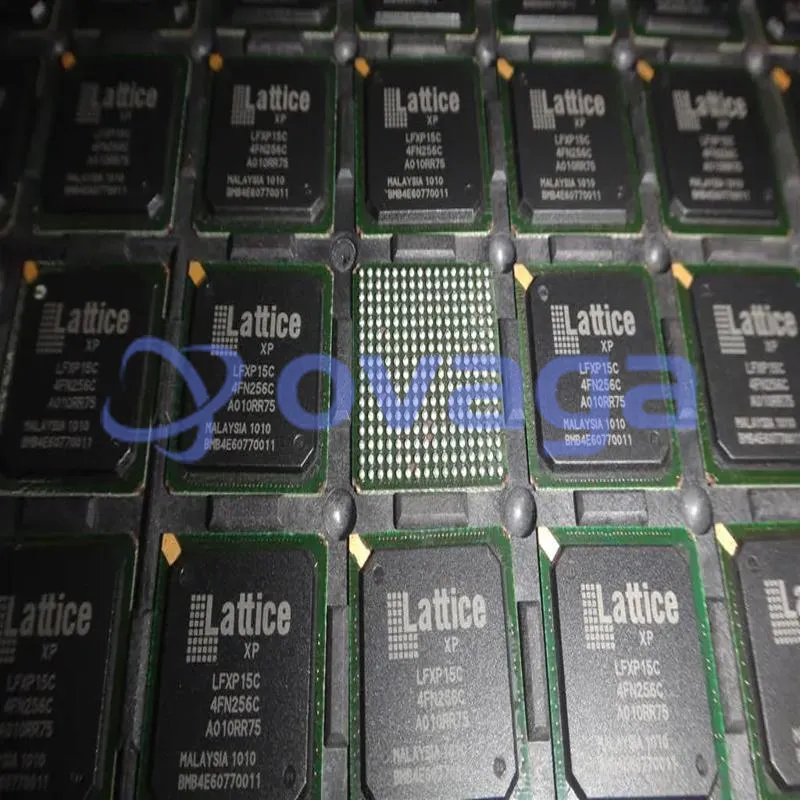
$5000LFXP15C-4FN256C
High-speed FPGA with 15.4K LUTs and 188 IO


Brands: LATTICE SEMICONDUCTOR CORP
Mfr.Part #: LFXP15C-4FN256C
Datasheet: LFXP15C-4FN256C Datasheet (PDF)
Package/Case: 256-FPBGA (17x17)
Product Type: FPGAs (Field Programmable Gate Array)
RoHS Status:
Stock Condition: 6,554 pcs, New Original
Warranty: 1 Year Ovaga Warranty - Find Out More
0
1
LFXP15C-4FN256C General Description
With its Flash*Freeze technology enabling rapid power-down and recovery, the LFXP15C-4FN256C facilitates enhanced energy efficiency in power-sensitive applications. Its advanced features, including pre-engineered source synchronous I/O support and on-chip PLLs, make it a versatile choice for diverse design requirements. Furthermore, its support for configuration via industry-standard interfaces such as SPI and I2C simplifies integration into various systems, making it an ideal FPGA solution for a wide range of applications
Specifications
| Parameter | Value | Parameter | Value |
|---|---|---|---|
| Pbfree Code | Yes | Rohs Code | Yes |
| Part Life Cycle Code | Obsolete | Ihs Manufacturer | LATTICE SEMICONDUCTOR CORP |
| Part Package Code | BGA | Package Description | 17 X 17 MM, 1 MM PITCH, LEAD FREE, PLASTIC, FPBGA-256 |
| Pin Count | 256 | Reach Compliance Code | not_compliant |
| ECCN Code | EAR99 | HTS Code | 8542.39.00.01 |
| Clock Frequency-Max | 375 MHz | Combinatorial Delay of a CLB-Max | 0.53 ns |
| JESD-30 Code | S-PBGA-B256 | JESD-609 Code | e1 |
| Length | 17 mm | Moisture Sensitivity Level | 3 |
| Number of CLBs | 1932 | Number of Inputs | 188 |
| Number of Logic Cells | 1932 | Number of Outputs | 188 |
| Number of Terminals | 256 | Operating Temperature-Max | 85 °C |
| Operating Temperature-Min | Organization | 1932 CLBS | |
| Package Body Material | PLASTIC/EPOXY | Package Code | BGA |
| Package Equivalence Code | BGA256,16X16,40 | Package Shape | SQUARE |
| Package Style | GRID ARRAY | Peak Reflow Temperature (Cel) | 250 |
| Power Supplies | 1.8/2.5/3.3 V | Programmable Logic Type | FIELD PROGRAMMABLE GATE ARRAY |
| Qualification Status | Not Qualified | Seated Height-Max | 2.1 mm |
| Supply Voltage-Max | 3.465 V | Supply Voltage-Min | 1.71 V |
| Supply Voltage-Nom | 1.8 V | Surface Mount | YES |
| Technology | CMOS | Temperature Grade | OTHER |
| Terminal Finish | Tin/Silver/Copper (Sn/Ag/Cu) | Terminal Form | BALL |
| Terminal Pitch | 1 mm | Terminal Position | BOTTOM |
| Time@Peak Reflow Temperature-Max (s) | 40 | Width | 17 mm |
| Manufacturer | Lattice | Product Category | FPGA - Field Programmable Gate Array |
| Shipping Restrictions | This product may require additional documentation to export from the United States. | RoHS | Details |
| Series | LFXP15C | Number of Logic Elements | 15000 LE |
| Embedded Memory | 324 kbit | Number of I/Os | 188 I/O |
| Supply Voltage - Min | 1.71 V | Supply Voltage - Max | 3.465 V |
| Minimum Operating Temperature | 0 C | Maximum Operating Temperature | + 85 C |
| Mounting Style | SMD/SMT | Package / Case | FPBGA-256 |
| Brand | Lattice | Distributed RAM | 61 kbit |
| Embedded Block RAM - EBR | 324 kbit | Maximum Operating Frequency | 360 MHz |
| Moisture Sensitive | Yes | Number of Logic Array Blocks - LABs | 1875 LAB |
| Operating Supply Voltage | 1.8 V/2.5 V/3.3 V | Product Type | FPGA - Field Programmable Gate Array |
| Factory Pack Quantity | 90 | Subcategory | Programmable Logic ICs |
| Total Memory | 385 kbit |
Shipping
| Shipping Type | Ship Fee | Lead Time | |
|---|---|---|---|
 |
DHL | $20.00-$40.00 (0.50 KG) | 2-5 days |
 |
Fedex | $20.00-$40.00 (0.50 KG) | 2-5 days |
 |
UPS | $20.00-$40.00 (0.50 KG) | 2-5 days |
 |
TNT | $20.00-$40.00 (0.50 KG) | 2-5 days |
 |
EMS | $20.00-$40.00 (0.50 KG) | 2-5 days |
 |
REGISTERED AIR MAIL | $20.00-$40.00 (0.50 KG) | 2-5 days |
Processing Time:Shipping fee depend on different zone and country.
Payment
| Terms of payment | Hand Fee | |
|---|---|---|
 |
Wire Transfer | charge US$30.00 banking fee. |
 |
Paypal | charge 4.0% service fee. |
 |
Credit Card | charge 3.5% service fee. |
 |
Western Union | charge US.00 banking fee. |
 |
Money Gram | charge US$0.00 banking fee. |
Guarantees
1.The electronic components you purchase include 365 Days Warranty, We guarantee product quality.
2.If some of the items you received aren't of perfect quality, we would resiponsibly arrange your refund or replacement. But the items must remain their orginal condition.
Packing
-

Step1 :Product
-

Step2 :Vacuum packaging
-

Step3 :Anti-static bag
-

Step4 :Individual packaging
-

Step5 :Packaging boxes
-

Step6 :bar-code shipping tag


All the products will packing in anti-staticbag. Ship with ESD antistatic protection.
Outside ESD packing’s lable will use ourcompany’s information: Part Mumber, Brand and Quantity.
We will inspect all the goods before shipment,ensure all the products at good condition and ensure the parts are new originalmatch datasheet.
After all the goods are ensure no problems afterpacking, we will packing safely and send by global express. It exhibitsexcellent puncture and tear resistance along with good seal integrity.


Part points
-
The LFXP15C-4FN256C is a field-programmable gate array (FPGA) chip produced by Lattice Semiconductor. It belongs to the LatticeXP2 family and features 15,000 LUTs, 240 kbits of embedded memory, and 144 user I/Os. With its low power consumption and high performance, it's suitable for a variety of applications including industrial control, automotive, and consumer electronics.
-
Equivalent
The LFXP15C-4FN256C chip is an FPGA (Field-Programmable Gate Array). Equivalent products include Altera (now Intel) Cyclone IV EP4CE15 or Xilinx Spartan-6 XC6SLX16. These offer similar functionality and performance. -
Features
The LFXP15C-4FN256C is an FPGA (Field-Programmable Gate Array) from Lattice Semiconductor. It features 15,000 LUTs (Look-Up Tables), 6 multipliers, and 128 I/O pins. With its compact 256-pin package, it offers flexibility and high-performance for various applications like embedded systems, communication, and industrial automation. -
Pinout
The LFXP15C-4FN256C is a FPGA (Field Programmable Gate Array) with 256 pins. It includes non-volatile Flash memory and features 15,000 Look-Up Tables and 360 Kbits of RAM. The device can be reprogrammed and configured to perform various digital logic functions. -
Manufacturer
The manufacturer of the LFXP15C-4FN256C is Lattice Semiconductor Corporation. Lattice Semiconductor is a leading provider of programmable logic devices, field-programmable gate arrays (FPGAs), design software, IP cores, and reference designs. They are known for their innovative solutions in communications, computing, industrial, automotive, and consumer markets. -
Application Field
The LFXP15C-4FN256C is typically used in applications such as handheld devices, consumer electronics, industrial automation, and automotive systems. It is commonly utilized for functions such as signal processing, interface control, data encryption, and power management due to its low power consumption and small form factor. -
Package
The LFXP15C-4FN256C chip is a Field-Programmable Gate Array (FPGA) available in a 256-ball FineLine BGA package. It belongs to the LatticeXP2 family, offering 15,000 Look-Up Tables (LUTs) and various features for customizable logic solutions.


We provide high quality products, thoughtful service and after sale guarantee
-

We have rich products, can meet your various needs.
-

Minimum order quantity starts from 1pcs.
-

Lowest international shipping fee starts from $0.00
-

365 days quality guarantee for all products


