


Images are for reference only See Product Specifications
Orders Over
$5000ORT8850L-2BMN680C
A flexible and efficient solution for FPGA-based system design and implementatio


Brands: Lattice Semiconductor Corporation
Mfr.Part #: ORT8850L-2BMN680C
Datasheet: ORT8850L-2BMN680C Datasheet (PDF)
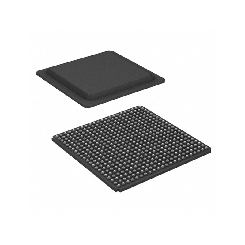
Package/Case: 680-BBGA
Product Type: FPGAs (Field Programmable Gate Array)
RoHS Status:
Stock Condition: 5,056 pcs, New Original
Warranty: 1 Year Ovaga Warranty - Find Out More
0
1
ORT8850L-2BMN680C General Description
Additionally, this module incorporates advanced features such as overcurrent protection, thermal shutdown, and overvoltage protection, ensuring reliable operation and safeguarding against potential damage to connected components. Furthermore, its high efficiency and low dropout voltage characteristics contribute to minimizing power loss and maximizing energy efficiency, making it ideal for battery-powered applications where power consumption is critical
Features
- Embedded Core Features
- Implemented in an ORCA Series 4 FPGA.
- Allows a wide range of high-speed backplane applications, including SONET transport and termination.
- No knowledge of SONET/SDH needed in generic applications. Simply supply data, 78 MHz—106 MHz clock, and a frame pulse.
- High-Speed Interface (HSI) function for clock/data recovery serial backplane data transfer without external clocks.
- Eight-channel HSI function provides 850 Mbits/s serial interface per channel for a total chip bandwidth of 6.8 Gbits/s (full duplex).
- HSI function uses Lattice’s 850 Mbits/s serial interface core. Rates from 126 Mbits/s to 850 Mbits/s are supported.
- LVDS I/Os compliant with EIA®-644 support hot insertion. All embedded LVDS I/Os include both input and output on-board termination to allow long-haul driving of backplanes.
- Low-power 1.5 V HSI core.
- Low-power LVDS buffers.
- Programmable STS-3, and STS-12 framing.
- Independent STS-3, and STS-12 data streams per quad channels.
- 8:1 data multiplexing/demultiplexing for 106.25 MHz byte-wide data processing in FPGA logic.
- On-chip, Phase-Lock Loop (PLL) clock meets (type B) jitter tolerance specification of ITU-T recommendation G.958.
- Powerdown option of HSI receiver on a per-channel basis.
- HSI automatically recovers from loss-of-clock once its reference clock returns to normal operating state.
- Frame alignment across multiple ORT8850 devices for work/protect switching at OC-192/STM-64 and above rates.
- In-band management and configuration through transport overhead extraction/insertion.
- Supports transparent modes where either the only insertion is A1/A2 framing bytes, or no bytes are inserted.
- Streamlined pointer processor (pointer mover) for 8 kHz frame alignment to system clocks.
- Built-in boundry scan (IEEE ®1149.1 JTAG).
- FIFOs align incoming data across all eight channels (two groups of four channels or four groups of two channels) for both SONET scrambling. Optional ability to bypass alignment FIFOs.
- 1 + 1 protection supports STS-12/STS-48 redundancy by either software or hardware control for protection switching applications. STS-192 and above rates are supported through multiple devices.
- ORCA FPGA soft intellectual property core support for a variety of applications.
- Programmable Synchronous Transport Module (STM) pointer mover bypass mode.
- Programmable STM framer bypass mode.
- Programmable Clock and Data Recovery (CDR) bypass mode (clocked LVDS High-Speed Interface).
- Redundant outputs and multiplexed redundant inputs for CDR I/Os allow for implementation of eight channels with redundancy on a single device.
Specifications
| Parameter | Value | Parameter | Value |
|---|---|---|---|
| Series | ORCA® 4 | Package | Tray |
| Product Status | Obsolete | Programmabe | Not Verified |
| Number of Logic Elements/Cells | 4992 | Total RAM Bits | 75776 |
| Number of I/O | 278 | Number of Gates | 397000 |
| Voltage - Supply | 1.425V ~ 3.6V | Mounting Type | Surface Mount |
| Operating Temperature | 0°C ~ 70°C (TA) | Package / Case | 680-BBGA |
| Supplier Device Package | 680-FPBGA (35x35) |
Shipping
| Shipping Type | Ship Fee | Lead Time | |
|---|---|---|---|
 |
DHL | $20.00-$40.00 (0.50 KG) | 2-5 days |
 |
Fedex | $20.00-$40.00 (0.50 KG) | 2-5 days |
 |
UPS | $20.00-$40.00 (0.50 KG) | 2-5 days |
 |
TNT | $20.00-$40.00 (0.50 KG) | 2-5 days |
 |
EMS | $20.00-$40.00 (0.50 KG) | 2-5 days |
 |
REGISTERED AIR MAIL | $20.00-$40.00 (0.50 KG) | 2-5 days |
Processing Time:Shipping fee depend on different zone and country.
Payment
| Terms of payment | Hand Fee | |
|---|---|---|
 |
Wire Transfer | charge US$30.00 banking fee. |
 |
Paypal | charge 4.0% service fee. |
 |
Credit Card | charge 3.5% service fee. |
 |
Western Union | charge US.00 banking fee. |
 |
Money Gram | charge US$0.00 banking fee. |
Guarantees
1.The electronic components you purchase include 365 Days Warranty, We guarantee product quality.
2.If some of the items you received aren't of perfect quality, we would resiponsibly arrange your refund or replacement. But the items must remain their orginal condition.
Packing
-

Step1 :Product
-

Step2 :Vacuum packaging
-

Step3 :Anti-static bag
-

Step4 :Individual packaging
-

Step5 :Packaging boxes
-

Step6 :bar-code shipping tag


All the products will packing in anti-staticbag. Ship with ESD antistatic protection.
Outside ESD packing’s lable will use ourcompany’s information: Part Mumber, Brand and Quantity.
We will inspect all the goods before shipment,ensure all the products at good condition and ensure the parts are new originalmatch datasheet.
After all the goods are ensure no problems afterpacking, we will packing safely and send by global express. It exhibitsexcellent puncture and tear resistance along with good seal integrity.


We provide high quality products, thoughtful service and after sale guarantee
-

We have rich products, can meet your various needs.
-

Minimum order quantity starts from 1pcs.
-

Lowest international shipping fee starts from $0.00
-

365 days quality guarantee for all products


